Ic 7483 Pin Diagram Circuit

Orpha Cremin

343logic-design-lab-manual-10 esl38-3rd-sem-2011 Solved: at the option of your instructor, use circuit simulation s 7483 instructor adder simulation

343logic-design-lab-manual-10 esl38-3rd-sem-2011

343logic-design-lab-manual-10 esl38-3rd-sem-2011

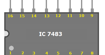
Adder bit ic 7483 using binary parallel adders four explain ques10 Truth applications etechnog Ic 7483 pin diagram, truth table, applications

Ic 7483 pin diagram, truth table, applications

Ic adder bit 7483 binary using pooja joshi parallel descriptionDesign and explain 8 bit binary adder using ic 7483. Manual logic 7483 icDesign and explain 8 bit binary adder using ic 7483..

Solved the diagram and results table for the 7483 adder is .

Solved: At the option of your instructor, use circuit simulation s

IC 7483 Pin Diagram, Truth Table, Applications - ETechnoG

Solved The diagram and results table for the 7483 adder is | Chegg.com

Design and explain 8 bit binary adder using IC 7483.

IC 7483 Pin Diagram, Truth Table, Applications - ETechnoG

343logic-design-lab-manual-10 esl38-3rd-sem-2011

Design and explain 8 bit binary adder using IC 7483.


YOU MIGHT ALSO LIKE